In the relentless pursuit of smaller, faster, and more powerful electronic devices, the industry has hit a thermal wall. As components shrink, the heat they generate becomes more concentrated, creating “thermal bottlenecks” that traditional materials simply cannot handle. For engineers and product managers, the challenge is clear: how do you maintain high performance without sacrificing the lifespan of the device?
The answer lies in the substrate. While standard organic laminates like FR-4 have served the industry for decades, the shift toward high-power density has made Ceramic Printed Circuit Boards (PCBs) the new gold standard.
At Smartlink Engineering, we understand that selecting the right material is only half the battle. Successful implementation requires a partner who can bridge the gap between complex material science and scalable manufacturing. Communicating and coordinating with Smartlink Engineering corporate services is the most effective way to ensure your next-generation power systems are built on a foundation of reliability and precision.
The Thermal Conductivity Gap: Why FR-4 Falls Short
The primary role of a PCB substrate is to provide electrical insulation while mechanical supporting components. However, in modern power electronics—such as EV inverters, LED arrays, and industrial motor drives—the substrate must also act as a primary heat sink.
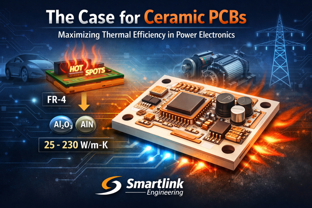
Traditional FR-4 is essentially a composite of glass fiber and epoxy resin. While cost-effective, it is a thermal insulator. Its thermal conductivity typically sits around 0.25 W/m·K. When a high-power component is mounted on FR-4, the heat stays trapped near the component, leading to localized “hot spots.” These hot spots accelerate the aging of semiconductor junctions and can cause catastrophic failure of solder joints.
In contrast, ceramic materials offer a leap in performance:
- Alumina ($Al_2O_3$): Offers thermal conductivity between 20 and 30 W/m·K, roughly 100 times that of FR-4.
- Aluminum Nitride ($AlN$): Reaches staggering levels of 170 to 230 W/m·K, providing thermal dissipation properties that rival metals while maintaining high electrical insulation.
By switching to ceramic, designers can often eliminate bulky external fans or heavy copper heat spreaders, allowing for the “compact power cooler” systems that modern aerospace and automotive sectors demand.
Beyond Heat: The Mechanical Advantages of Ceramics
Thermal management isn’t the only reason to move toward ceramic substrates. Reliability in harsh environments depends heavily on how materials behave when they get hot.
1. Coefficient of Thermal Expansion (CTE) Matching
Every material expands when heated. The problem occurs when the PCB expands at a different rate than the silicon chips mounted to it. This mismatch creates mechanical stress on the solder balls, eventually leading to cracks.
Ceramic substrates have a CTE (approx. 2.6 to 6 ppm/°C) that very closely matches silicon. This “CTE matching” ensures that the entire assembly expands and contracts in unison, significantly extending the fatigue life of the device in applications subject to rapid thermal cycling.
2. High Dielectric Strength and Isolation
Ceramics are naturally superior insulators. They can withstand significantly higher voltages than organic boards without the risk of electrical tracking or dielectric breakdown. This makes them indispensable for high-voltage applications where safety and isolation are non-negotiable.
3. Hermeticity and Chemical Resistance
Unlike FR-4, which can absorb moisture over time, ceramics are completely non-porous. They are immune to water absorption and highly resistant to chemical corrosion, making them the ideal choice for medical implants, deep-sea exploration tools, and sensors exposed to industrial chemicals.
Specialization in Ceramic Manufacturing Technologies
Not all ceramic PCBs are created equal. Depending on your power requirements and budget, different metallization techniques are utilized. Understanding these nuances is where Smartlink Engineering’s expertise becomes an asset to your design team.
- Direct Bonded Copper (DBC): In this process, a sheet of copper is fused to the ceramic substrate in a high-temperature furnace. This creates a bond with zero thermal interface resistance, perfect for high-current power modules.
- Active Metal Brazing (AMB): Used primarily with high-performance ceramics like Silicon Nitride ($Si_3N_4$), AMB uses a specialized brazing alloy to create an incredibly strong bond. This technology is the backbone of the latest Electric Vehicle (EV) power electronics due to its ability to survive extreme thermal shocks.
- Thick Film Technology: Conductive pastes are screen-printed onto the ceramic and “fired” at high temperatures. This is a versatile and cost-effective method for sensors and automotive electronics.
Why Partner with Smartlink Engineering?
The transition to ceramic-based systems involves sophisticated engineering hurdles. Sourcing the material is one thing; assembling it into a functional, tested, and reliable module is another.
Smartlink Engineering provides a comprehensive suite of corporate services tailored to these high-stakes projects. By coordinating with our team, you gain:
- Supply Chain Stability: Based in Malaysia’s primary industrial hubs (Shah Alam and Penang), we provide a secure, localized supply chain for global markets, mitigating the risks of geopolitical volatility.
- Design for Manufacturability (DFM): We don’t just build what you draw; we analyze your designs to ensure they are optimized for the best yield and performance, often identifying potential failure points before they reach the factory floor.
- One-Stop Integration: From component sourcing and precision PCBA to final functional testing and system integration, we manage the entire lifecycle. This “one-stop” approach reduces lead times and ensures that accountability for quality rests with a single, trusted partner.
The most successful projects are those that begin with a conversation. Coordinating with Smartlink Engineering corporate services allows your company to leverage over two decades of experience in the semiconductor and electronics manufacturing services (EMS) industry.
Frequently Asked Questions (FAQ)
Q: Is a ceramic PCB always better than a metal core PCB (MCPCB)?
While MCPCBs use a metal base (like Aluminum) to help with heat, they still require a thin polymer dielectric layer between the copper and the metal. This layer acts as a thermal barrier. Ceramic PCBs do not need this layer, as the substrate itself is both the insulator and the conductor of heat, offering much higher efficiency.
Q: Are ceramic PCBs brittle?
While ceramics are rigid, when properly mounted within a housing or module, they offer exceptional structural integrity. Advanced ceramics like Silicon Nitride also offer much higher fracture toughness compared to standard Alumina, making them suitable for high-vibration environments.
Q: How does Smartlink Engineering ensure quality for high-power applications?
We employ rigorous testing protocols, including Automated Optical Inspection (AOI), X-ray inspection for solder voids, and full functional testing. Our facilities are geared toward the precision required by the automotive and medical sectors.
Q: Can I use ceramic PCBs for high-frequency RF applications?
Yes. Ceramics have very low dielectric loss at high frequencies, which means they maintain signal integrity much better than organic substrates. This makes them a top choice for 5G infrastructure and radar systems.
Q: What is the first step to starting a project with Smartlink?
The best way to start is by reaching out to our corporate services team through our website. We can assist with everything from initial feasibility studies to full-scale production planning.
Conclusion
As the electronics industry moves toward more compact, power-dense solutions, the move to ceramic substrates is no longer optional—it is a competitive necessity. By choosing a partner like Smartlink Engineering, you aren’t just buying a component; you are investing in a sophisticated engineering ecosystem designed to handle the toughest thermal challenges of the 21st century.